
10.6: Ejercicios
- Page ID
- 83400

\( \newcommand{\vecs}[1]{\overset { \scriptstyle \rightharpoonup} {\mathbf{#1}} } \)
\( \newcommand{\vecd}[1]{\overset{-\!-\!\rightharpoonup}{\vphantom{a}\smash {#1}}} \)
\( \newcommand{\id}{\mathrm{id}}\) \( \newcommand{\Span}{\mathrm{span}}\)
( \newcommand{\kernel}{\mathrm{null}\,}\) \( \newcommand{\range}{\mathrm{range}\,}\)
\( \newcommand{\RealPart}{\mathrm{Re}}\) \( \newcommand{\ImaginaryPart}{\mathrm{Im}}\)
\( \newcommand{\Argument}{\mathrm{Arg}}\) \( \newcommand{\norm}[1]{\| #1 \|}\)
\( \newcommand{\inner}[2]{\langle #1, #2 \rangle}\)
\( \newcommand{\Span}{\mathrm{span}}\)
\( \newcommand{\id}{\mathrm{id}}\)
\( \newcommand{\Span}{\mathrm{span}}\)
\( \newcommand{\kernel}{\mathrm{null}\,}\)
\( \newcommand{\range}{\mathrm{range}\,}\)
\( \newcommand{\RealPart}{\mathrm{Re}}\)
\( \newcommand{\ImaginaryPart}{\mathrm{Im}}\)
\( \newcommand{\Argument}{\mathrm{Arg}}\)
\( \newcommand{\norm}[1]{\| #1 \|}\)
\( \newcommand{\inner}[2]{\langle #1, #2 \rangle}\)
\( \newcommand{\Span}{\mathrm{span}}\) \( \newcommand{\AA}{\unicode[.8,0]{x212B}}\)
\( \newcommand{\vectorA}[1]{\vec{#1}} % arrow\)
\( \newcommand{\vectorAt}[1]{\vec{\text{#1}}} % arrow\)
\( \newcommand{\vectorB}[1]{\overset { \scriptstyle \rightharpoonup} {\mathbf{#1}} } \)
\( \newcommand{\vectorC}[1]{\textbf{#1}} \)
\( \newcommand{\vectorD}[1]{\overrightarrow{#1}} \)
\( \newcommand{\vectorDt}[1]{\overrightarrow{\text{#1}}} \)
\( \newcommand{\vectE}[1]{\overset{-\!-\!\rightharpoonup}{\vphantom{a}\smash{\mathbf {#1}}}} \)
\( \newcommand{\vecs}[1]{\overset { \scriptstyle \rightharpoonup} {\mathbf{#1}} } \)
\( \newcommand{\vecd}[1]{\overset{-\!-\!\rightharpoonup}{\vphantom{a}\smash {#1}}} \)
\(\newcommand{\avec}{\mathbf a}\) \(\newcommand{\bvec}{\mathbf b}\) \(\newcommand{\cvec}{\mathbf c}\) \(\newcommand{\dvec}{\mathbf d}\) \(\newcommand{\dtil}{\widetilde{\mathbf d}}\) \(\newcommand{\evec}{\mathbf e}\) \(\newcommand{\fvec}{\mathbf f}\) \(\newcommand{\nvec}{\mathbf n}\) \(\newcommand{\pvec}{\mathbf p}\) \(\newcommand{\qvec}{\mathbf q}\) \(\newcommand{\svec}{\mathbf s}\) \(\newcommand{\tvec}{\mathbf t}\) \(\newcommand{\uvec}{\mathbf u}\) \(\newcommand{\vvec}{\mathbf v}\) \(\newcommand{\wvec}{\mathbf w}\) \(\newcommand{\xvec}{\mathbf x}\) \(\newcommand{\yvec}{\mathbf y}\) \(\newcommand{\zvec}{\mathbf z}\) \(\newcommand{\rvec}{\mathbf r}\) \(\newcommand{\mvec}{\mathbf m}\) \(\newcommand{\zerovec}{\mathbf 0}\) \(\newcommand{\onevec}{\mathbf 1}\) \(\newcommand{\real}{\mathbb R}\) \(\newcommand{\twovec}[2]{\left[\begin{array}{r}#1 \\ #2 \end{array}\right]}\) \(\newcommand{\ctwovec}[2]{\left[\begin{array}{c}#1 \\ #2 \end{array}\right]}\) \(\newcommand{\threevec}[3]{\left[\begin{array}{r}#1 \\ #2 \\ #3 \end{array}\right]}\) \(\newcommand{\cthreevec}[3]{\left[\begin{array}{c}#1 \\ #2 \\ #3 \end{array}\right]}\) \(\newcommand{\fourvec}[4]{\left[\begin{array}{r}#1 \\ #2 \\ #3 \\ #4 \end{array}\right]}\) \(\newcommand{\cfourvec}[4]{\left[\begin{array}{c}#1 \\ #2 \\ #3 \\ #4 \end{array}\right]}\) \(\newcommand{\fivevec}[5]{\left[\begin{array}{r}#1 \\ #2 \\ #3 \\ #4 \\ #5 \\ \end{array}\right]}\) \(\newcommand{\cfivevec}[5]{\left[\begin{array}{c}#1 \\ #2 \\ #3 \\ #4 \\ #5 \\ \end{array}\right]}\) \(\newcommand{\mattwo}[4]{\left[\begin{array}{rr}#1 \amp #2 \\ #3 \amp #4 \\ \end{array}\right]}\) \(\newcommand{\laspan}[1]{\text{Span}\{#1\}}\) \(\newcommand{\bcal}{\cal B}\) \(\newcommand{\ccal}{\cal C}\) \(\newcommand{\scal}{\cal S}\) \(\newcommand{\wcal}{\cal W}\) \(\newcommand{\ecal}{\cal E}\) \(\newcommand{\coords}[2]{\left\{#1\right\}_{#2}}\) \(\newcommand{\gray}[1]{\color{gray}{#1}}\) \(\newcommand{\lgray}[1]{\color{lightgray}{#1}}\) \(\newcommand{\rank}{\operatorname{rank}}\) \(\newcommand{\row}{\text{Row}}\) \(\newcommand{\col}{\text{Col}}\) \(\renewcommand{\row}{\text{Row}}\) \(\newcommand{\nul}{\text{Nul}}\) \(\newcommand{\var}{\text{Var}}\) \(\newcommand{\corr}{\text{corr}}\) \(\newcommand{\len}[1]{\left|#1\right|}\) \(\newcommand{\bbar}{\overline{\bvec}}\) \(\newcommand{\bhat}{\widehat{\bvec}}\) \(\newcommand{\bperp}{\bvec^\perp}\) \(\newcommand{\xhat}{\widehat{\xvec}}\) \(\newcommand{\vhat}{\widehat{\vvec}}\) \(\newcommand{\uhat}{\widehat{\uvec}}\) \(\newcommand{\what}{\widehat{\wvec}}\) \(\newcommand{\Sighat}{\widehat{\Sigma}}\) \(\newcommand{\lt}{<}\) \(\newcommand{\gt}{>}\) \(\newcommand{\amp}{&}\) \(\definecolor{fillinmathshade}{gray}{0.9}\)10.6.1: Problemas de análisis
1. Para el circuito de la Figura\(\PageIndex{1}\), determinar\(I_D\) y\(V_{DS}\). \(I_{DSS}\)= 40 mA,\(V_{GS(off)}\) = −4 V,\(V_{DD}\) = 26 V,\(V_{GG}\) = −2 V,\(R_G\) = 220 k\(\Omega\),\(R_D\) = 1.2 k\(\Omega\).
2. Para el circuito de la Figura\(\PageIndex{1}\), determinar\(I_D\) y\(V_{DS}\). \(I_{DSS}\)= 20 mA,\(V_{GS(off)}\) = −3 V,\(V_{DD}\) = 22 V,\(V_{GG}\) = −1 V,\(R_G\) = 390 k\(\Omega\),\(R_D\) = 1 k\(\Omega\).
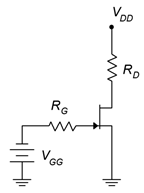
Figura\(\PageIndex{1}\)
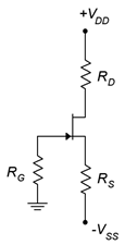
3. Para el circuito de la Figura\(\PageIndex{2}\), determinar\(I_D\),\(V_G\) y\(V_D\). \(I_{DSS}\)= 24 mA,\(V_{GS(off)}\) = −6 V,\(V_{DD}\) = 36 V,\(R_G\) = 220 k\(\Omega\),\(R_S\) = 2 k\(\Omega\),\(R_D\) = 1.8 k\(\Omega\).
4. Para el circuito de la Figura\(\PageIndex{2}\), determinar\(I_D\),\(V_S\) y\(V_{DS}\). \(I_{DSS}\)= 18 mA,\(V_{GS(off)}\) = −3 V,\(V_{DD}\) = 30 V,\(R_G\) = 270 k\(\Omega\),\(R_S\) = 2.7 k\(\Omega\),\(R_D\) = 3.3 k\(\Omega\).

Figura\(\PageIndex{2}\)
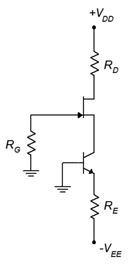
5. Para Figura\(\PageIndex{3}\), determinar\(I_D\),\(V_G\) y\(V_D\). \(I_{DSS}\)= 16 mA,\(V_{DD}\) = 25 V,\(V_{GS(off)}\) = −3 V,\(V_{SS}\) = −6 V,\(R_G\) = 560 k\(\Omega\),\(R_S\) = 2 k\(\Omega\),\(R_D\) = 3.6 k\(\Omega\).
6. Para Figura\(\PageIndex{3}\), determinar\(I_D\), y\(V_{DS}\). \(I_{DSS}\)= 16 mA,\(V_{DD}\) = 25 V,\(V_{GS(off)}\) = −3 V,\(V_{SS}\) = −9 V,\(R_G\) = 680 k\(\Omega\),\(R_S\) = 2 k\(\Omega\),\(R_D\) = 2.7 k\(\Omega\).
Figura\(\PageIndex{3}\)
7. Para Figura\(\PageIndex{4}\), determinar\(I_D\),\(V_G\) y\(V_D\). \(I_{DSS}\)= 16 mA,\(V_{DD}\) = 25 V,\(V_{GS(off)}\) = −3 V,\(V_{EE}\) = −9 V,\(R_G\) = 810 k\(\Omega\),\(R_E\) = 2 k\(\Omega\),\(R_D\) = 2.7 k\(\Omega\).
8. Para el circuito de la Figura\(\PageIndex{4}\), determinar\(I_D\) y\(V_{DS}\). \(I_{DSS}\)= 40 mA,\(V_{GS(off)}\) = −4 V,\(V_{DD}\) = 30 V,\(V_{EE}\) = −6 V,\(R_G\) = 750 k\(\Omega\),\(R_E\) = 500\(\Omega\),\(R_D\) = 1.8 k\(\Omega\).
10.6.2: Problemas de diseño
9. Usando el circuito de la Figura\(\PageIndex{2}\), determine un valor\(R_S\)\(I_D\) para establecer en 4 mA. \(I_{DSS}\)= 10 mA,\(V_{GS(off)}\) = −2 V,\(V_{DD}\) = 20 V,\(R_G\) = 430 k\(\Omega\),\(R_D\) = 1.8 k\(\Omega\).
10. Usando el circuito de la Figura\(\PageIndex{1}\), determine un valor\(V_{GG}\)\(I_D\) para establecer en 2 mA. \(I_{DSS}\)= 10 mA,\(V_{GS(off)}\) = −4 V,\(V_{DD}\) = 28 V,\(R_G\) = 470 k\(\Omega\),\(R_D\) = 4.7 k\(\Omega\).
11. Usando el circuito de la Figura\(\PageIndex{4}\), determine un valor\(R_E\)\(I_D\) para establecer en 4 mA. \(I_{DSS}\)= 18 mA,\(V_{GS(off)}\) = −3 V,\(V_{DD}\) = 25 V,\(V_{EE}\) = −12 V,\(R_G\) = 330 k\(\Omega\),\(R_D\) = 2.2 k\(\Omega\).
Figura\(\PageIndex{4}\)
12. Usando el circuito de la Figura\(\PageIndex{4}\), se determinan los valores\(R_D\) para\(R_E\) y\(I_D\) para establecer en 5 mA y\(V_D\) en 6 V.\(I_{DSS}\) = 20 mA,\(V_{GS(off)}\) = −4 V,\(V_{DD}\) = 32 V,\(V_{EE}\) = −10 V,\(R_G\) = 390 k\(\Omega\).
10.6.3: Problemas de desafío
13. Siguiendo la derivación de la Ecuación 10.4.2, derivar la Ecuación 10.4.4.
14. Usando el circuito de la Figura\(\PageIndex{3}\), determine los valores para\(R_S\) y\(V_{SS}\)\(I_D\) para establecer en 4 mA. \(I_{DSS}\)= 16 mA,\(V_{GS(off)}\) = −4 V,\(V_{DD}\) = 30 V,\(R_G\) = 680 k\(\Omega\),\(R_D\) = 2 k\(\Omega\).
10.6.4: Problemas de simulación por computadora
15. Realizar una simulación de punto de funcionamiento de CC en el circuito del Problema 7 para verificar los resultados. El J111 será suficiente.
16. Realizar una simulación de punto de funcionamiento de CC en el circuito del Problema 10 para verificar los resultados. El J111 será suficiente.
10.6.5: Departamento de Utilidad Marginal
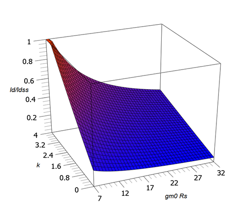
Figura\(\PageIndex{5}\): Gráfico de superficie de sesgo combinado.
Las gráficas de la Figura 10.4.13 representan tres cortes de esta superficie.
Se ve genial, pero...